Hardware
Version 1.0
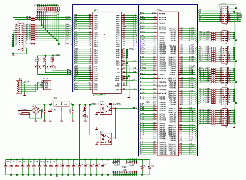
Schematic of the miniLA is shown on the picture below.

Heart of the miniLA is CPLD XC95288XL from Xilinx. This reprogrammable devices implements all of the logic.
Samples are stored into fast synchronous SRAM. Schematic and PCB shows original memory CY7C1347.
However, memory AS7C33128 was finally used instead. It required modification of firmware and grounding of currently disconnected pins 64(ZZ) and
14(FT) ![]() picture.
Care must be taken when choosing some other memory, because it might not be fully compatible. For example original memory CY7C1347 works in pipelined mode, but flow-through mode of AS7C33128 is used here.
picture.
Care must be taken when choosing some other memory, because it might not be fully compatible. For example original memory CY7C1347 works in pipelined mode, but flow-through mode of AS7C33128 is used here.
Devices are supplied by 3.3V stabilized by LD1117DT-3.3.
Oscillator IC4(IC6) is clock source for the CPLD. This oscillator is supplied by 3.3V. Good source for oscillators are old PC mainboards. Experiences shown, that such oscillators did not have problem to work with 3.3V power supply although they were designed for 5V.
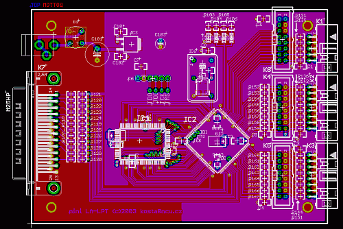
Next picture shows the PCB layout. Dual layered PCB uses mix design combining both thru-hole and SMD devices.

Important note:
For the EMC reasons, the connections
between JTAG pins of the CPLD and the connector K6 are not made and wires need to be added ![]() picture.
picture.
Errata
- Vss connects to pin 39 of the SRAM instead of 40. Solution - connect pins 39 and 40 (pin 39 is not used by SRAM).
Downloads:
Schematic: ![]() PDF
PDF
Whole package (schematic, device placement): ![]() ZIP
ZIP