Mainboard
Version 1.1
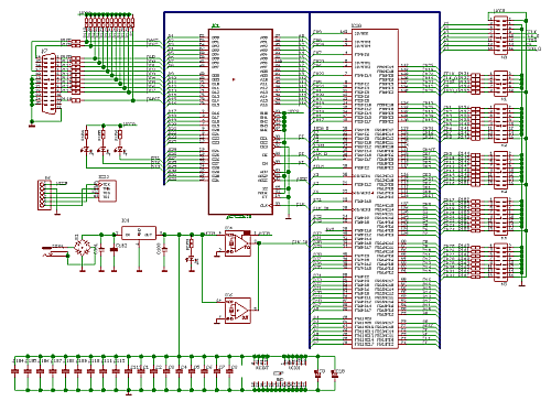
Schematic of the miniLA is shown on the picture below.

Heart of the miniLA is CPLD XC95288XL from Xilinx. This reprogrammable devices implements all of the necessary logic.
Samples are stored into fast synchronous SRAM AS7C33128.
Devices are supplied by 3.3V stabilized by LD1117DT-3.3.
Oscillator IC4(IC6) is a clock source for the CPLD. This oscillator is supplied by 3.3V. Good source for oscillators are old PC mainboards. Experiences shown, that such oscillators did not have problem to work with 3.3V power supply, although they are designed for 5V.
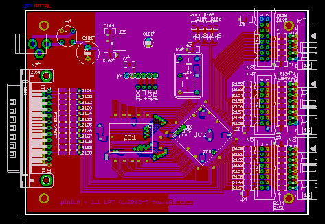
Next picture shows the PCB layout. Dual layered PCB uses thru-hole and SMD devices.

Important note:
For the EMC reasons, the connections
between JTAG pins of the CPLD and the connector K6 are not made and wires need to be added ![]() picture.
picture.
Errata
- Vss connects to pin 39 of the SRAM instead of 40. Solution - connect pins 39 and 40 (pin 39 is not used by SRAM).
Changelog
Version 1.1
- Modified for memory AS7C33128, (removed bits D32-D34, inputs FT and ZZ grounded).
- Added thermals for easier soldering.
- Corrected orientation of LED diodes on the PCB.
- Signal names on schematic renamed to be in accordance with firmware 1.6 and 2.1.
Downloads
Schematic: ![]() PDF
PDF
Whole package (schematic, device placement, Gerber, Excellon and PS data for PCB): ![]() ZIP
ZIP
XC9500XL Family datasheet: ![]() PDF
PDF
Fast synchronous SRAM AS7C33128 datasheet: ![]() PDF
PDF